LED Module PCB Pad Repair Guide
A professional guide to repairing lifted, burned, missing, or cracked PCB pads on LED display modules, including fault diagnosis, pad reconstruction, jumper routing, solder control, testing, and when a module should be replaced instead of repaired.
PCB-Level LED Module Repair
LED Module PCB Pad Repair Guide
Lifted pads, burned pads, broken traces, and cracked vias are common after impact, water damage, overheating, or repeated LED bead replacement. A reliable repair is possible, but only when the damaged copper path is understood before solder is added.
Inspect
Find whether the pad, via, trace, LED, or driver output is actually open.
Expose
Remove solder mask only where a reliable copper connection is needed.
Bridge
Use the shortest safe jumper route that does not disturb the LED mask.
Test
Verify RGB, grayscale, thermal stability, and vibration before reinstalling.
1. Confirm the Pad Is the Real Failure Point
A dark pixel after lamp-bead replacement is often blamed on the LED, but a damaged pad can produce the same symptom. Before rebuilding copper, compare the suspect pixel with a known-good neighboring pixel using continuity, diode mode, and visual inspection under magnification.
Check whether the pad is completely missing, partially lifted, cracked around a via, carbonized from overheating, or disconnected from its trace. The repair method changes depending on which failure you find.
| Damage type | Typical cause | Best repair direction |
|---|---|---|
| Pad edge lifted | Excessive force while removing an LED | Flatten and secure if copper is still connected; avoid pulling it further |
| Pad missing | Overheated pad or forced component removal | Rebuild connection with a fine jumper to the nearest confirmed copper node |
| Cracked via | Impact, flexing, moisture, or thermal stress | Bridge around the via after confirming both sides of the circuit |
| Burned/carbonized area | Short circuit, wrong voltage, or prolonged overheating | Remove conductive carbon, inspect insulation, and consider module replacement |
| Trace broken under solder mask | Scratch, corrosion, or repeated repair | Expose clean copper and bridge with insulated wire |
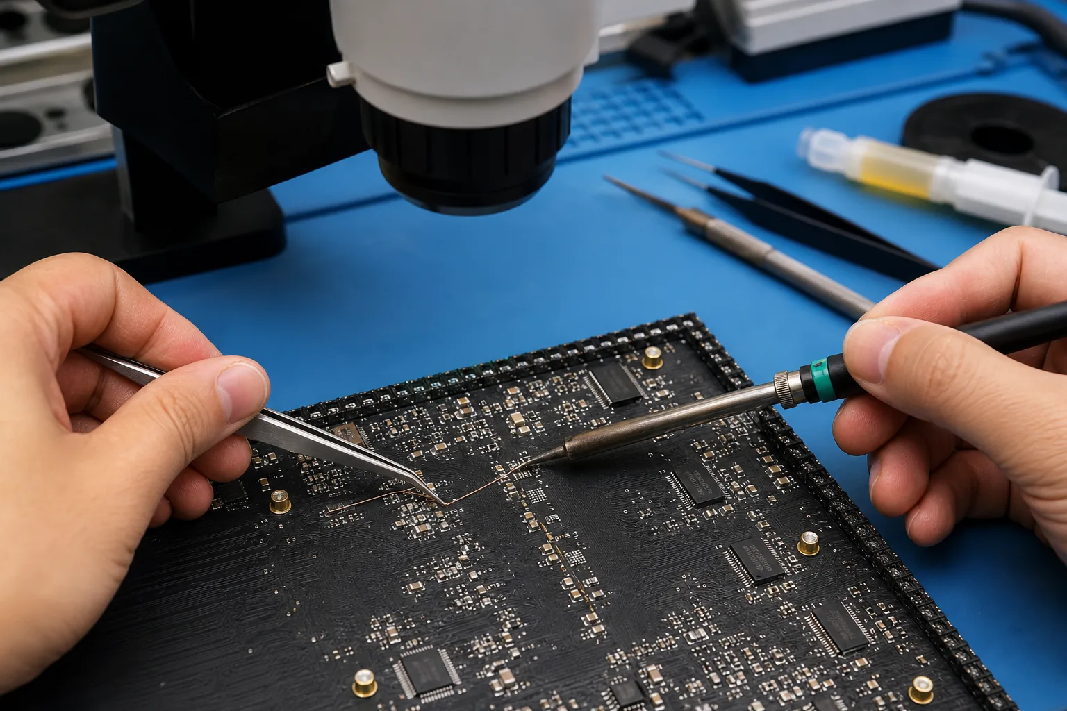
2. Tools and Materials
- Microscope or high-magnification inspection camera
- Fine-tip soldering iron with stable temperature control
- Hot-air station for LED removal only when needed
- 0.02–0.08 mm enamelled copper wire or fine insulated jumper wire
- Flux, low-temperature solder, solder wick, precision tweezers
- Fiberglass pen, micro blade, or controlled scraping tool for solder mask
- UV solder mask, conformal coating, or suitable electronics adhesive for strain relief
- Digital multimeter and LED module test card
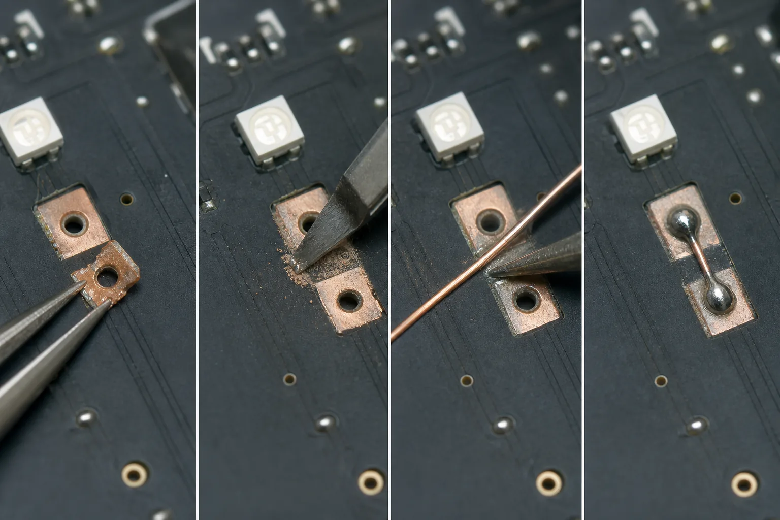
3. Repair Workflow for a Missing LED Pad
- Map the circuit. Identify where the missing pad originally connected. Use an identical neighboring LED circuit as a reference.
- Clean the damage. Remove loose copper, burned flux, and solder balls. Do not enlarge the damaged area unnecessarily.
- Expose copper carefully. Scrape a small section of the connected trace or via until bright copper appears. Avoid cutting adjacent traces.
- Tin the copper. Add flux and a minimal amount of solder. The goal is wetting, not building a large solder mound.
- Prepare the jumper. Use a short, mechanically stable wire route. Keep it low enough that the LED mask or module face will not press on it.
- Solder one side first. Anchor the wire to the exposed copper, then verify continuity before connecting to the LED pad area.
- Install the LED. Place the LED with correct polarity and solder the remaining pads with balanced solder volume.
- Strain-relieve the repair. Secure the jumper with UV solder mask or suitable coating after electrical testing.
Professional tip: a jumper that works electrically but sits too high can create a visible bump, mask interference, or long-term failure from pressure. Keep the repair path flat and protected.
4. Pad Repair Quality Standards
Electrical
Continuity is stable, no shorts exist between RGB channels, and the repaired pixel follows the same behavior as neighboring pixels.
Mechanical
The LED sits flat, the jumper is secured, and gentle vibration or thermal cycling does not break the connection.
Optical
The pixel brightness, color, viewing angle, and black-body appearance match the surrounding module.
Serviceability
The repair is clean enough that future inspection, module mask installation, and maintenance remain possible.
5. When a Pad Repair Is Not Worth It
Do not force a board-level repair when the PCB is carbonized, multilayer vias are destroyed, corrosion is widespread, multiple adjacent pads are missing, or the repaired area will sit under mechanical pressure. In those cases, replacing the LED module is usually safer than creating an unstable field repair.
Final Checklist
- RGB channels light independently and correctly.
- No short exists between adjacent pads or channels.
- The jumper route is short, flat, insulated, and strain-relieved.
- The LED body is level with neighboring pixels.
- Full white and low-gray patterns are stable after warm-up.
- The repair survives light tap and flex testing without flicker.
PCB pad repair is one of the most delicate LED module repairs. The best results come from patient circuit tracing, minimal solder volume, and strong mechanical protection after the electrical connection is restored.