How to Replace LED Lamp Beads on P2.5 / P3.9 LED Modules
A step-by-step guide to replacing damaged SMD LED lamp beads on P2.5 and P3.9 LED display modules, including component matching, polarity, hot-air settings, pad preparation, alignment, reflow, and final color testing.
Fine-Pitch Module Repair
How to Replace LED Lamp Beads on P2.5 / P3.9 LED Modules
P2.5 and P3.9 modules are common in indoor rental screens, stage displays, fixed installations, conference rooms, and commercial LED walls. Their SMD lamp beads are replaceable, but the tight spacing leaves little room for excess heat, solder, or alignment error.
A successful repair depends on using the correct LED, preserving the PCB pads, and matching the repaired pixel with the surrounding module.
P2.5
Often uses compact black-body SMD packages such as 2121 or similar, depending on the module design.
P3.9
Indoor versions commonly use 2121-style packages; outdoor modules may use larger high-brightness packages such as 1921.
Critical Rule
Pixel pitch alone does not identify the LED. Match the package, polarity, brightness, color coordinates, and viewing angle.
1. Identify the Correct Replacement LED
Do not order replacement beads only by “P2.5 LED” or “P3.9 LED.” Different manufacturers use different SMD packages, polarity arrangements, chips, brightness bins, wavelengths, and black-body colors.
| Parameter | What must match | Why it matters |
|---|---|---|
| Package size | For example 2121, 2020, 1921, or the exact original footprint | Incorrect size will not align with the PCB pads |
| Polarity / pin layout | Common anode or common cathode and the exact RGB pin positions | A wrong layout can short channels or prevent the LED from lighting |
| Brightness and wavelength bin | Prefer the original production batch or a confirmed compatible batch | Mismatched pixels remain visible after repair |
| Body and lens color | Black-body depth, surface finish, and lens shape | Affects screen contrast and off-axis appearance |
| Indoor / outdoor grade | Protection, brightness, UV resistance, and moisture performance | Outdoor P3.9 modules have different environmental requirements |
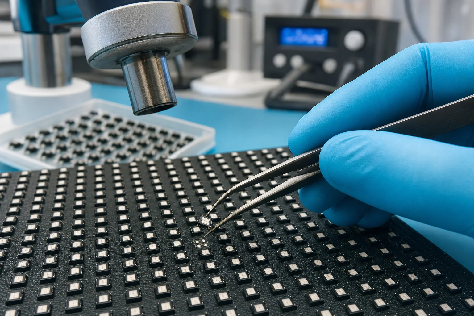
2. Prepare the Module and Workstation
- Disconnect all power and signal cables.
- Remove masks, coatings, or protective hardware without damaging neighboring pixels.
- Use an ESD-safe mat and wrist strap.
- Secure the PCB flat so it does not flex during heating.
- Inspect the rear side for plastic connectors or components that may be affected by heat.
- Record the LED orientation with a close-up photograph.
Temperature note: hot-air station readings are not the same as the temperature at the solder joint. Nozzle size, airflow, distance, board thickness, preheating, and calibration all change the real result. Start conservatively and use only enough heat to release the solder.
3. Remove the Damaged Lamp Bead
- Apply a very small amount of no-clean or suitable electronics flux around the LED.
- Shield adjacent LEDs if the nozzle or airflow is wide.
- Heat the component evenly from above. Avoid pushing it before the solder has fully melted.
- When the bead moves freely, lift it vertically with fine tweezers.
- Stop heating immediately after removal to reduce PCB discoloration and pad damage.
If the LED does not release quickly, do not increase force. Recheck the airflow, nozzle position, and solder condition. Pulling a partially molten component is one of the most common causes of lifted pads.
4. Clean and Inspect the PCB Pads
Use flux and fine solder wick to remove excess solder. The pads should be flat, intact, and similar in height. Clean the area and inspect it under magnification.
If a pad is missing, trace its circuit before attempting a jumper repair. A poorly routed wire can interfere with the module mask or create an unstable connection. For severely damaged fine-pitch boards, replacing the module may be more reliable than extensive pad reconstruction.
5. Place and Reflow the New LED
- Add a controlled, equal amount of solder to each pad.
- Confirm the replacement LED polarity a second time.
- Place the LED at the exact center of the pad pattern.
- Align its body with the neighboring pixel grid, not only with the solder pads.
- Reheat evenly until the solder wets and surface tension settles the package.
- Remove the heat and hold the board still while the joints solidify.
Too much solder
The LED floats above its neighbors, tilts, bridges channels, or shifts when cooling.
Too little solder
The joint may look connected but become intermittent during vibration or thermal cycling.
Excessive airflow
Nearby 2121/1921 LEDs can rotate, move, or develop disturbed solder joints.
Excessive heat time
Can damage the LED encapsulation, black-body finish, PCB mask, vias, and neighboring components.
6. Test the Repaired P2.5 / P3.9 Module
Before reinstalling the mask, connect the module to a controlled test system. Run the following patterns:
- Red, green, and blue independently
- Full white at low, medium, and high brightness
- Grayscale gradients, especially dark gray
- Horizontal and vertical line patterns
- Moving video or scrolling text to expose intermittent connections
View the module from the front and from several side angles. A replacement can be electrically correct but still show a brightness, wavelength, black-body, or angle mismatch.
7. Common Problems After Replacement
| Problem | Likely cause | Corrective action |
|---|---|---|
| One color remains off | Wrong pin layout, incomplete joint, damaged pad, or failed driver channel | Verify polarity and trace continuity to the driver IC |
| Pixel is brighter or darker | Different brightness or wavelength bin | Use a better-matched LED batch |
| Pixel color changes from the side | LED is tilted or has a different lens structure | Re-align or replace with the correct package |
| Neighboring pixels fail | Heat or airflow disturbed adjacent joints | Inspect and reflow only the affected joints |
| Pixel flickers after warm-up | Cold joint, insufficient solder, cracked trace, or thermal driver fault | Inspect under heat and compare the circuit with a good pixel |
8. When Not to Repair the Lamp Bead
Replace the complete module if the PCB is carbonized, multiple pads are missing, the board is warped, many LEDs have inconsistent aging, water corrosion is widespread, or the module uses a sealed COB/GOB construction that cannot be serviced reliably with normal SMD tools.
Final Thoughts
Replacing LED lamp beads on P2.5 and P3.9 modules is precise work. The key is not maximum heat or speed—it is controlled energy, correct component matching, accurate alignment, and disciplined testing.
Keep known-good replacement LEDs from the original module batch whenever possible. That single habit greatly reduces visible color differences and repeat repairs on professional LED display projects.